MAX2700/MAX2701
1.8GHz to 2.5GHz Direct Downconversion
Receivers
2 _______________________________________________________________________________________
ABSOLUTE MAXIMUM RATINGS
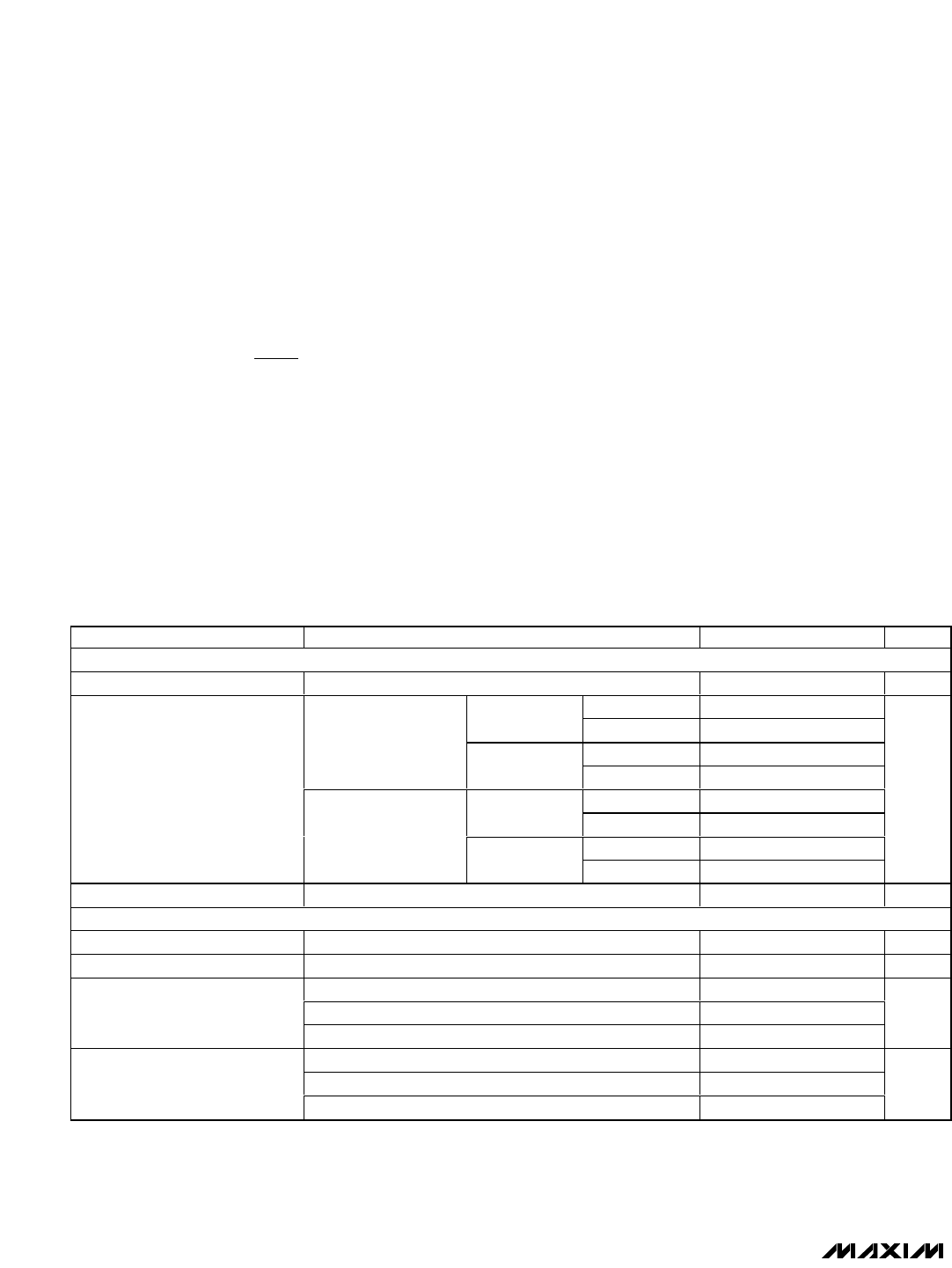
DC ELECTRICAL CHARACTERISTICS
(MAX2700/MAX2701 EV kit (Figure 3), V
CC
= +2.7V to +3.3V, SHDN = GAIN_SET = V
CC
, X2_EN = GND, V
AGC
= 1.25V, CEXT+ con-
nected to CEXT-; no RF input signals applied; RFIN, LNAIN, LO inputs are terminated with 50Ω, LNAOUT connected to V
CC
through a
10nH inductor; MIX_I, MIX_Q, QIN1+, QIN1-, QOUT1, IIN1+, IIN1-, IOUT1, QIN2+, QIN2-, QOUT2, IIN2+, IIN2-, IOUT2 pins are
unconnected; T
A
= -40°C to +85°C, unless otherwise noted. Typical values are at V
CC
= +3.0V, T
A
= +25°C.)
Stresses beyond those listed under “Absolute Maximum Ratings” may cause permanent damage to the device. These are stress ratings only, and functional
operation of the device at these or any other conditions beyond those indicated in the operational sections of the specifications is not implied. Exposure to
absolute maximum rating conditions for extended periods may affect device reliability.
V
CC
to GND..............................................................-0.3V to +6V
RF Signals
P
RFIN
, P
LNAIN
, P
LO
.....................................................+15dBm
Baseband Signals
IIN1+ to IIN1-, IIN2+ to IIN2-,
QIN1+ to QIN1-, QIN2+ to QIN2-......................................±2V
Input Voltages
AGC, GAIN_SET, SHDN, X2_EN
,
CEXT_, RFIN_, LO, LNAIN, IIN_ _,
QIN_ _ , DCI_ _ , DCQ_ _ to GND..........-0.3V to (V
CC
+ 0.3V)
Input Current
AGC……………………………………………………..±50mA
All Digital Inputs………………………………………..±10mA
Continuous Power Dissipation (T
A
= +70°C)
48-Pin TQFP-EP (derate 27mW/°C above +70°C).....2000mW
Operating Temperature Range ...........................-40°C to +85°C
Storage Temperature Range.............................-65°C to +150°C
Junction Temperature......................................................+150°C
Lead Temperature (soldering, 10s).................................+300°C

 (11 stránky)
 Manymanuals.com
 Manymanuals.de
 Manymanuals.fr
 Manymanuals.it
 Manymanuals.pl
 Manymanuals.cz
 Manymanuals.es
 Manymanuals-pt.com
Komentáře k této Příručce